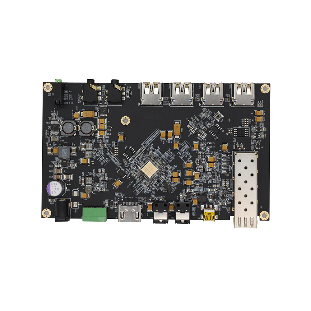
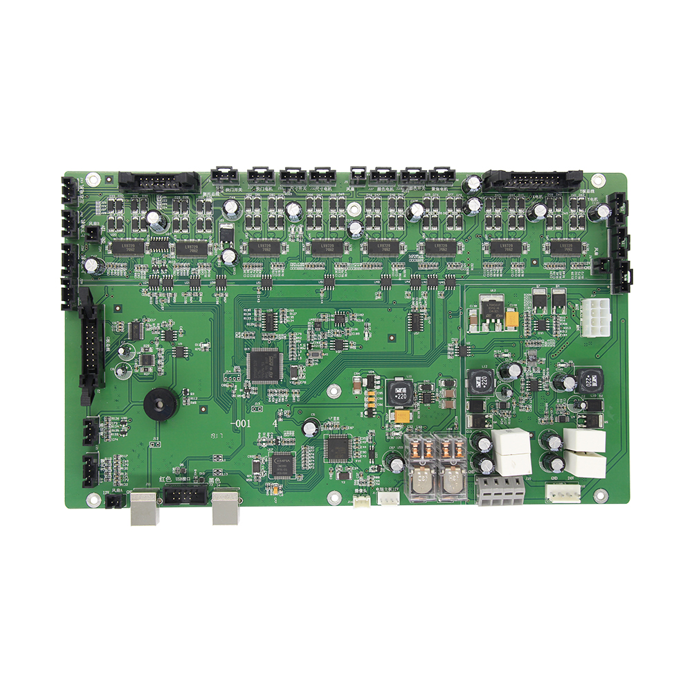
Electronic PCB Design Factory (EDF) has recently announced the launch of their state-of-the-art facility for designing, manufacturing, and testing printed circuit boards (PCBs). The company, known for its expertise in PCB manufacturing, has expanded its capabilities with the new facility, setting a new standard for quality and efficiency in the industry.EDF's new facility spans over 10,000 square feet and is equipped with the latest technology and machinery for PCB design and production. The facility is designed to streamline the entire process from initial concept to final product, allowing for faster turnaround times and superior quality control."We are thrilled to announce the opening of our new PCB design and manufacturing facility," said a spokesperson for EDF. "This expansion represents our commitment to innovation and excellence in the electronic manufacturing industry. With our new facility, we are better positioned to meet the growing demand for high-quality PCBs across various industries."The facility boasts advanced design software and hardware, allowing EDF's team of experienced engineers to create intricate and customized PCB layouts. Using cutting-edge technology, EDF is able to produce PCBs with high precision and accuracy, meeting the stringent requirements of their clients.One of the key features of the new facility is its focus on sustainability and environmental responsibility. EDF has invested in eco-friendly manufacturing processes and materials, ensuring that their operations have minimal impact on the environment. By implementing green practices, the company aims to lead the way in environmentally conscious PCB manufacturing.In addition to their advanced design and manufacturing capabilities, EDF has also integrated comprehensive testing and inspection processes into their facility. Every PCB undergoes rigorous testing to ensure functionality, durability, and reliability. This commitment to quality assurance sets EDF apart as a leader in the industry.With the opening of the new facility, EDF is poised to take on larger and more complex projects, catering to the evolving needs of their clients. The company has built a reputation for delivering high-quality PCBs on time and within budget, and the new facility will enable them to further solidify their position as a trusted partner for electronic manufacturing solutions."We are confident that our new facility will allow us to better serve our clients and exceed their expectations," said the spokesperson. "We look forward to leveraging our expanded capabilities to drive innovation and growth in the electronic manufacturing industry."As EDF continues to expand its operations, the company remains dedicated to fostering strong relationships with their clients. They understand the importance of collaboration and open communication, and they are committed to working closely with their clients to deliver tailored solutions that meet their specific needs.The launch of EDF's new PCB design and manufacturing facility represents a significant milestone for the company and the industry as a whole. With their unwavering dedication to quality, innovation, and sustainability, EDF is well-positioned to lead the way in electronic manufacturing for years to come.
Read More